| CPC H01L 23/53266 (2013.01) [H01L 23/5226 (2013.01); H01L 23/5286 (2013.01); H01L 23/53238 (2013.01); H01L 23/53252 (2013.01)] | 19 Claims |
|
1. A semiconductor device comprising:
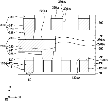
a first level wiring disposed at a first metal level, the first level wiring including a first line wiring, a first insulating capping film, and a first side wall graphene film, the first insulating capping film extending along and contacting an upper surface of the first line wiring, and the first side wall graphene film extending along and contacting a side wall of the first line wiring;
an interlayer insulating film which covers the side wall of the first line wiring and a side wall of the first insulating capping film; and
a second level wiring disposed at a second metal level higher than the first metal level, the second level wiring including a second via connected to the first line wiring, and a second line wiring connected to the second via,
wherein the second via penetrates the first insulating capping film,
wherein the interlayer insulating film contacts the side wall of the first insulating capping film, and
wherein the first insulating capping film does not extend along an upper surface of the interlayer insulating film.
|