| CPC H01L 23/5286 (2013.01) [H01L 21/76895 (2013.01); H01L 23/5283 (2013.01); H01L 25/071 (2013.01); H01L 27/092 (2013.01)] | 18 Claims |

|
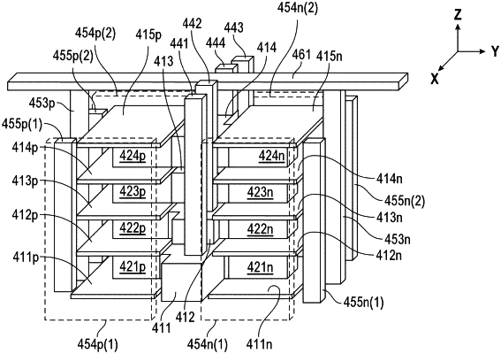
1. A method for forming a semiconductor apparatus, comprising:
forming a plurality of repetitive initial structures over a substrate of the semiconductor apparatus wherein an initial structure in the plurality of repetitive initial structures is formed by:
forming a first stack of transistors along a Z direction substantially perpendicular to a substrate plane, including:
forming a first transistor on the substrate, the first transistor formed with a first gate and a first channel surrounded by the first gate;
forming a second transistor over the first transistor along the Z direction, the second transistor formed with a second gate and a second channel surrounded by the second gate;
forming local interconnect structures, each of the transistors in the first stack of transistors being sandwiched between two of the local interconnect structures;
forming vertical conductive structures substantially parallel to the Z direction, a height of one of the vertical conductive structures along the Z direction being at least a height of the initial structure; and
forming the first stack of transistors as a stack of vertical field-effect transistors (VFETs), a current between a source and a drain of each of the VFETs transistors flowing substantially along the Z direction; and
forming a second stack of transistors adjacent to the first stack of transistors along the Z direction, including:
forming a third transistor on the substrate, the third transistor formed with a third gate and a third channel surrounded by the third gate;
forming a fourth transistor over the third transistor along the Z direction, the fourth transistor formed with a fourth gate and a fourth channel surrounded by the fourth gate;
functionalizing the initial structure into a final structure by forming one or more connections each electrically coupling one of the local interconnect structures to one of the vertical conductive structures;
forming a first gate connection structure electrically coupling a first gate of the first transistor with a third gate of the third transistor; and
forming a second gate connection structure electrically coupling a second gate of the second transistor with a fourth gate of the fourth transistor.
|