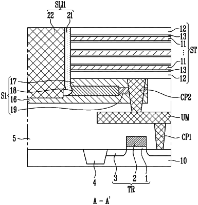
| CPC H01L 23/5226 (2013.01) [H01L 23/481 (2013.01); H10B 41/10 (2023.02); H10B 41/27 (2023.02); H10B 41/35 (2023.02); H10B 43/10 (2023.02); H10B 43/27 (2023.02); H10B 43/35 (2023.02)] | 19 Claims |

|
1. A semiconductor device comprising:
a line;
a source structure on the line;
a contact plug penetrating the source structure;
a stack structure on the source structure and the contact plug, wherein a lower surface of the stack structure is in contact with an upper surface of the contact plug;
a first slit structure penetrating the stack structure, extending in a first direction, and being adjacent to the contact plug in the first direction; and
a second slit structure penetrating the stack structure and extending in the first direction, the second slit structure being adjacent to the first slit structure in a second direction intersecting the first direction and being adjacent to the contact plug in the second direction,
wherein the first slit structure and the second slit structure are spaced apart from each other by a first distance in the second direction, the first slit structure and the contact plug are spaced apart from each other by a second distance in the first direction,
wherein the second distance is longer than the first distance, and
wherein a sidewall of the first slit structure and a sidewall of the contact plug face each other.
|
|
12. A semiconductor device comprising:
a line;
a source structure on the line;
a contact plug penetrating the source structure;
a stack structure on the source structure and the contact plug, wherein a lower surface of the stack structure is in contact with an upper surface of the contact plug; and
a first slit structure including a first penetration part penetrating the stack structure and extending in a first direction, and a first protrusion part protruding in the first direction toward the contact plug more than a sidewall of the first penetration part through the source structure,
wherein the contact plug is electrically connected to the line and is spaced apart from the first protrusion part, and
wherein the first protrusion part is positioned between the first penetration part and the contact plug.
|