| CPC H01L 23/49822 (2013.01) [H01L 21/4857 (2013.01); H01L 23/3121 (2013.01); H01L 23/49816 (2013.01); H01L 23/49827 (2013.01); H01L 23/562 (2013.01); H01L 25/16 (2013.01); H01L 25/50 (2013.01)] | 20 Claims |
|
1. A method of forming a chip package structure, the method comprising:
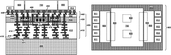
forming a combination of an interposer core assembly and a package-side redistribution structure over a carrier substrate, wherein the interposer core assembly comprises at least one silicon substrate interposer and a molding compound interposer frame that surrounds the at least one silicon substrate interposer, wherein one of the at least one silicon substrate interposer comprises metal bonding structures which are topmost components of vertical signal paths that vertically extend through said one of the at least one silicon substrate interposer;
forming a die-side redistribution structure comprising die-side redistribution wiring interconnects over the interposer core assembly, where the die-side redistribution wiring interconnects comprise via structures that are formed directly on surfaces of the metal bonding structures; and
attaching at least two semiconductor dies to the die-side redistribution structure, wherein a first subset of die-side redistribution wiring interconnects within the die-side redistribution structure provides chip-to-chip signal paths between the at least two semiconductor dies.
|