| CPC H01L 23/49816 (2013.01) [H01L 23/3128 (2013.01); H01L 23/49822 (2013.01); H01L 23/49838 (2013.01); H01L 24/04 (2013.01); H01L 24/16 (2013.01); H01L 2224/0401 (2013.01); H01L 2224/16227 (2013.01)] | 20 Claims |

|
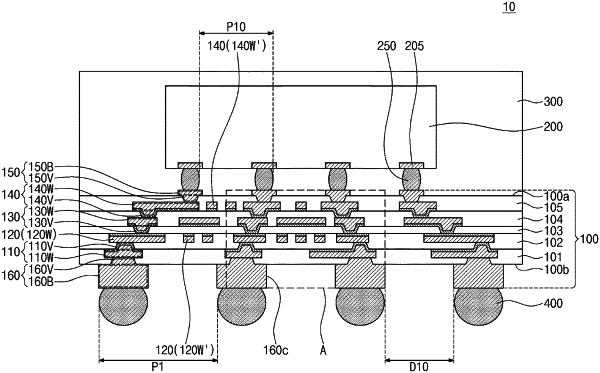
1. A semiconductor package, comprising:
a redistribution substrate; and
a semiconductor chip disposed on a top surface of the redistribution substrate,
wherein the redistribution substrate comprises:
an insulating layer; and
a first redistribution pattern, a second redistribution pattern, and a third redistribution pattern disposed in the insulating layer,
wherein the first to third redistribution patterns are sequentially stacked in a direction from a bottom surface of the redistribution substrate toward the top surface and are electrically connected to each other,
wherein each of the first to third redistribution patterns includes a wire portion that extends in a direction parallel to the top surface of the redistribution substrate,
each of the first and third redistribution patterns further includes a via portion that extends from the wire portion in a direction perpendicular to the top surface of the redistribution substrate,
the second redistribution pattern further comprises first fine wire patterns that are less wide than the wire portion of the second redistribution pattern,
wherein a distance between adjacent first fine wire patterns ranges from 0.5 μm to 2 μm,
a width of the via portion of the first redistribution pattern is smallest at a level of a top surface of the via portion of the first redistribution pattern, and
a width of the via portion of the third redistribution pattern is smallest at a level of a bottom surface of the via portion of the third redistribution pattern.
|