| CPC H01L 23/142 (2013.01) [H01L 23/4827 (2013.01); H01L 23/49827 (2013.01)] | 11 Claims |
|
1. A semiconductor package, comprising:
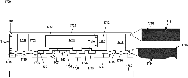
an electrically insulating core having a first side, a second side opposite the first side and configured for mounting to a substrate, and an electrically conductive first via extending through a periphery region of the core, the periphery region defining an opening in the core, the core comprising glass fibres interwoven with epoxy material, the core having one or more regions at the second side where the glass fibres are exposed from the epoxy material;
a power semiconductor die embedded in the opening in the core, the power semiconductor die being thinner than the core and comprising a first load terminal bond pad at a first side which faces a same direction as the first side of the core, a second load terminal bond pad at a second side which faces a same direction as the second side of the core, and a control terminal bond pad at the first side or the second side of the power semiconductor die;
a resin in the opening in the core and that encases the power semiconductor die;
a first contact pad plated on the first via at the second side of the core; and
a second contact pad plated on the first load terminal bond pad of the power semiconductor die at the first side of the core.
|