| CPC H01L 21/76897 (2013.01) [H01L 21/28114 (2013.01); H01L 21/28247 (2013.01); H01L 21/3083 (2013.01); H01L 21/32139 (2013.01); H01L 21/76883 (2013.01); H01L 21/76885 (2013.01); H01L 21/76892 (2013.01); H01L 21/823431 (2013.01); H01L 21/823475 (2013.01); H01L 23/5283 (2013.01); H01L 29/41783 (2013.01); H01L 29/41791 (2013.01); H01L 29/42376 (2013.01); H01L 29/66545 (2013.01); H01L 29/66795 (2013.01); H01L 29/785 (2013.01)] | 19 Claims |

|
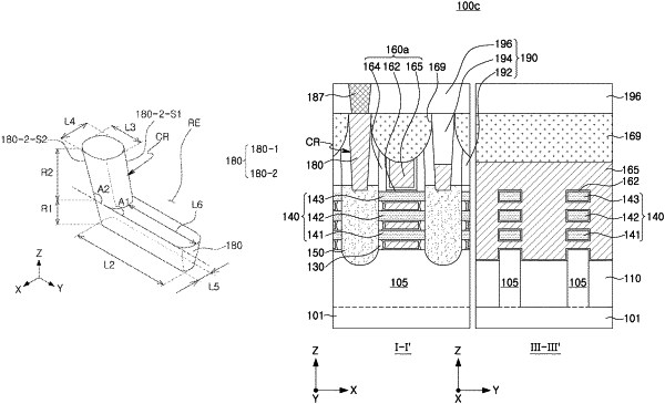
1. A semiconductor device, comprising:
an active region extending in a first direction on a substrate;
a gate electrode extending in a second direction to intersect the active region;
channel layers spaced apart from each other in a third direction, perpendicular to an upper surface of the substrate, on the active region and surrounded by the gate electrode;
source/drain regions on both sides of the gate electrode and connected to the channel layers;
an interlayer insulating layer covering the source/drain regions;
a contact plug penetrating through the interlayer insulating layer and connected to each of the source/drain regions,
wherein the contact plug includes a first portion extending in the second direction, and a second portion protruding upwardly from an end of the first portion and defining a recess region of the contact plug, and
wherein a first length of the second portion in the second direction is less than a second length of the recess region in the second direction; and
a contact insulating layer filling the recess region of the contact plug.
|
|
10. A semiconductor device, comprising:
an active region extending in a first direction on a substrate;
a gate electrode extending in a second direction to intersect the active region;
channel layers spaced apart from each other in a third direction, perpendicular to an upper surface of the substrate, on the active region and surrounded by the gate electrode;
source/drain regions on both sides of the gate electrode and connected to the channel layers;
a contact plug connected to each of the source/drain regions on each of the source/drain regions; and
a gate capping layer on the gate electrode and having a width greater than a width of the gate electrode,
wherein the contact plug includes a first portion extending in the second direction, and a second portion protruding upwardly from a portion of the first portion and defining at least one recess region of the contact plug, and
wherein a length of an upper surface of the second portion in the first direction is greater than a length of a lower surface of the first portion in the first direction.
|
|
15. A semiconductor device, comprising:
an active region extending in a first direction on a substrate;
a gate electrode extending in a second direction to intersect the active region;
source/drain regions on both sides of the gate electrode;
a contact plug connected to each of the source/drain regions;
a gate capping layer on the gate electrode and having a recessed edge in a shape recessed from an upper surface; and
a contact insulating layer filling the recessed edge of the gate capping layer,
wherein the contact plug includes a first portion extending in the second direction, and a second portion protruding upwardly from a portion of the first portion and defining at least one recess region of the contact plug, and
wherein the contact insulating layer fills the at least one recess region of the contact plug.
|