| CPC H01L 21/76816 (2013.01) [H01L 21/32139 (2013.01); H01L 21/76832 (2013.01); H01L 21/76879 (2013.01); H01L 23/5226 (2013.01); H01L 23/5283 (2013.01); H01L 23/53266 (2013.01)] | 11 Claims |

|
1. A method of manufacturing a semi-damascene structure of a semiconductor device, the method comprising:
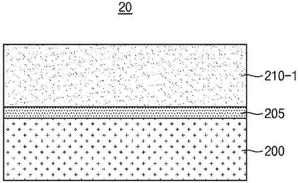
forming a 1st intermetal dielectric layer;
forming a 1st hardmask layer and at least one 1st photoresist pattern on the 1st intermetal dielectric layer;
patterning at least one via hole penetrating through the 1st hardmask layer and the 1st intermetal dielectric using the at least one 1st photoresist pattern;
removing the at least one 1st photoresist pattern;
forming a metal structure in the at least one via hole such that the metal structure fills in the at least one via hole and extends on the 1st hardmask layer;
patterning the metal structure to form at least one 1st trench penetrating at least the metal structure at a portion where the metal structure extends on the 1st hardmask layer; and
filling the at least one 1st trench with a 2nd intermetal dielectric layer.
|