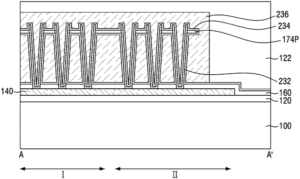
| CPC H01L 21/486 (2013.01) [H05K 3/107 (2013.01); H01L 23/642 (2013.01)] | 20 Claims |

|
1. A method of manufacturing an interposer, the method comprising:
providing a substrate including a first region and a second region adjacent to the first region;
forming a first mold structure on the substrate;
forming a photoresist layer on the first mold structure, the photoresist layer extending over the first region and the second region of the substrate;
forming a first transfer pattern over the photoresist layer on the first region, using a first photomask;
forming a second transfer pattern over the photoresist layer on the second region, using the first photomask;
forming a mask pattern on the first mold structure, using the first transfer pattern and the second transfer pattern; and
forming a first trench and a second trench in the first mold structure, using the mask pattern, the first trench being formed in the first region, and the second trench being formed in the second region,
forming a first conductive layer which covers an inner wall of the first trench and an inner wall of the second trench,
in each of the first trench and the second trench, the first conductive layer having an inner face facing a center of the first trench or the second trench, respectively, and an outer face facing away from the center of the first trench or second trench, respectively, the inner and outer faces being opposing faces of the first conductive layer;
forming a support structure extending between and contacting the outer face of the first conductive layer in the first trench to the outer face of the first conductive layer in the second trench;
forming a dielectric layer which covers the first conductive layer and the support structure, and, the dielectric layer contacting both the inner face of the first conductive layer and the outer face of the first conductive layer; and
forming a second conductive layer on the dielectric layer such that the second conductive layer is within both the first trench and the second trench, and is both above and below the support structure, and the dielectric layer is between the first and second conductive layers.
|