| CPC H01L 21/28568 (2013.01) [C23C 16/045 (2013.01); C23C 16/14 (2013.01); C23C 16/45527 (2013.01); C23C 16/45544 (2013.01); H01L 21/76805 (2013.01); H01L 21/76895 (2013.01); H01L 23/53209 (2013.01); H01L 23/53242 (2013.01); H01L 23/53257 (2013.01); H10B 41/27 (2023.02); H10B 43/27 (2023.02)] | 17 Claims |
|
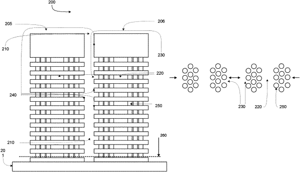
1. A method of filling a 3-D structure of a partially manufactured semiconductor substrate with a conductive material, the 3-D structure comprising sidewalls, a plurality of openings in the sidewalls leading to a plurality of features having a plurality of interior regions fluidically accessible through the openings, the method comprising:
depositing a first bulk layer of the conductive material within the 3-D structure such that the first bulk layer partially fills the plurality of interior regions of the 3-D structure;
depositing a second bulk layer of the conductive material within the 3-D structure on the first bulk layer such that the second bulk layer at least partially fills the plurality of interior regions of the 3-D structure; and
depositing a third bulk layer of the conductive material within the 3-D structure on the sidewalls, wherein the first bulk layer, second bulk layer, and third bulk layer are deposited at different conditions.
|