| CPC H01L 21/0332 (2013.01) [C23C 16/30 (2013.01); C23C 16/32 (2013.01); C23C 16/50 (2013.01); H01J 37/32449 (2013.01); H01J 37/32816 (2013.01); H01L 21/02115 (2013.01); H01L 21/02274 (2013.01); H01J 2237/332 (2013.01); H01L 21/02205 (2013.01); H01L 21/31122 (2013.01); H01L 21/31144 (2013.01)] | 20 Claims |
|
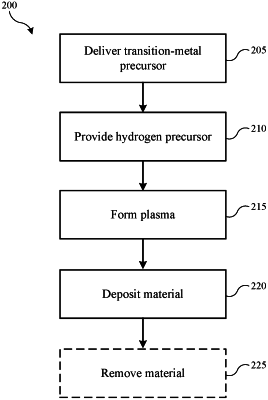
1. A deposition method comprising:
delivering a ruthenium-containing precursor and a hydrogen-containing precursor to a processing region of a semiconductor processing chamber, wherein at least one of the ruthenium-containing precursor or the hydrogen-containing precursor comprises carbon;
forming a plasma of all precursors within the processing region of a semiconductor processing chamber; and
depositing a ruthenium-and-carbon material on a substrate disposed within the processing region of the semiconductor processing chamber, wherein the ruthenium-and-carbon material is characterized by an as-deposited surface roughness of less than or about 1.0 nm.
|