| CPC H01L 21/02529 (2013.01) [C30B 29/36 (2013.01); H01L 21/02378 (2013.01); H01L 21/046 (2013.01); H01L 21/78 (2013.01); H01L 29/1608 (2013.01); H01L 29/34 (2013.01); H01L 29/66068 (2013.01); H01L 29/7802 (2013.01)] | 11 Claims |
|
1. A silicon carbide epitaxial substrate comprising:
a silicon carbide substrate; and
a silicon carbide epitaxial film located on the silicon carbide substrate, wherein
a main front surface of the silicon carbide epitaxial film includes an outer edge, an outer peripheral region located within 3 mm from the outer edge, and a central region surrounded by the outer peripheral region,
a maximum diameter of the main front surface is more than or equal to 150 mm,
the central region has one or more macroscopic defects,
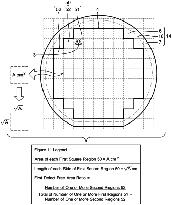
wherein when the central region is divided into a plurality of first square regions each having an area of A cm2, the plurality of first square regions have one or more first regions having the one or more macroscopic defects and one or more second regions not having the one or more macroscopic defects,
wherein when the central region is divided into a plurality of second square regions each having an area of B cm2, the plurality of second square regions have one or more third regions having the one or more macroscopic defects and one or more fourth regions not having the one or more macroscopic defects,
wherein when a value obtained by dividing the number of the one or more second regions by a total of the number of the one or more first regions and the number of the one or more second regions is defined as a first defect free area ratio, a value obtained by dividing the number of the one or more fourth regions by a total of the number of the one or more third regions and the number of the one or more fourth regions is defined as a second defect free area ratio, and a value obtained by dividing the number of the one or more macroscopic defects by an area of the central region is defined as X cm−2, A is smaller than B, B is less than or equal to 4, X is more than 0 and less than 4, and a Formula 1 is satisfied:
 wherein when Formula 1 is satisfied the macroscopic defects are more locally concentrated than when Formula 1 is not satisfied.
|