| CPC H01J 37/32669 (2013.01) [H01J 37/32146 (2013.01); H01J 37/3244 (2013.01); H01J 37/3266 (2013.01); H01J 37/32715 (2013.01); H01L 21/26 (2013.01); H01L 21/6831 (2013.01); H01J 2237/327 (2013.01)] | 16 Claims |
|
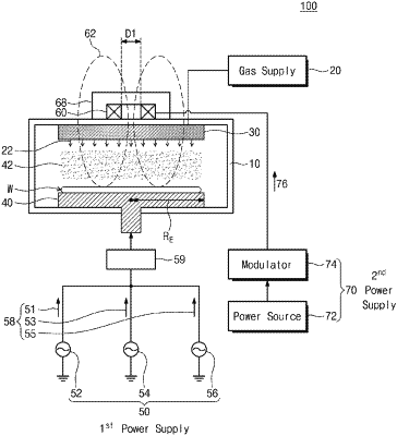
1. A method of fabricating a semiconductor device, the method comprising:
seating a substrate having a substrate radius on an electrostatic chuck;
applying first radio-frequency power to the electrostatic chuck to induce plasma in a region at least above the electrostatic chuck, wherein the first radio-frequency power is provided by a first radio-frequency power supply; and
generating a magnetic field in the region at least above the electrostatic chuck using a magnet having a ring-shape and disposed above the electrostatic chuck by applying second radio-frequency power to the magnet, wherein the second radio-frequency power is applied to the magnet by a second radio-frequency power supply including a power source generating a source voltage, and a modulator connected between the power source and the magnet, and wherein the modulator is configured to generate a pulse through modulation of the source voltage,
wherein the magnet has an inner radius ranging from about one-half to about one-fourth of the substrate radius,
wherein the modulator comprises:
a pulse generator configured to generate the pulse; and
a peak generator connected to the pulse generator and configured to generate a peak of the pulse,
wherein the pulse generator comprises:
first delay cells connected in series to the power source; and
a first gate driver connected to the first delay cells to provide a trigger signal to the first delay cells, and
wherein the peak generator comprises:
an additional power source;
second delay cells connected in series to the additional power source, and
a second gate driver connected to the first gate driver and the second delay of cells to provide the trigger signal to the second delay of cells.
|