| CPC H01J 37/10 (2013.01) [H01J 37/20 (2013.01); H01J 37/28 (2013.01)] | 20 Claims |
|
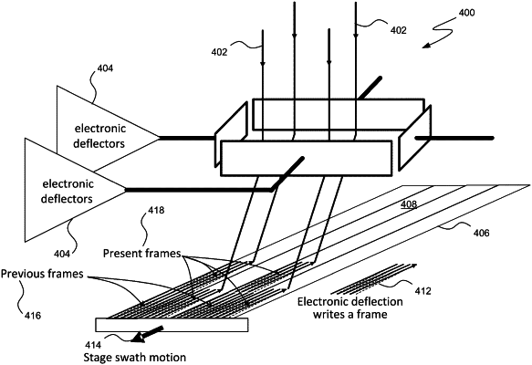
1. A system comprising:
an electron emitter source configured to emit an illumination beam;
a beam splitter lens array configured to split the illumination beam into multiple electron beams;
an electronic deflection system configured to deflect each of the electron beams in a plurality of directions, including a first direction, along two different axes; and
a swathing stage configured to move a sample during writing of scan lines by the electronic beams with a constant velocity in a second direction that is parallel to the first direction, wherein the scan lines are written parallel to the second direction in a rectangular pattern by each of the electron beams, wherein a length of the rectangular pattern is measured along the first direction and the length is longer than a width of the rectangular pattern.
|