| CPC G11C 11/419 (2013.01) [G11C 11/413 (2013.01); H03K 19/20 (2013.01)] | 7 Claims |
|
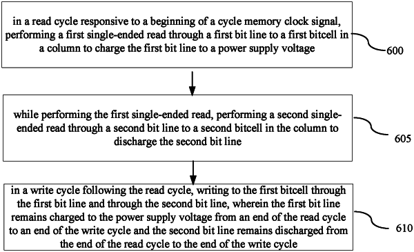
1. A method for a memory, comprising:
in a read cycle responsive to a beginning of a cycle memory clock signal, performing a first single-ended read through a first bit line to a first bitcell in a column to charge the first bit line to a power supply voltage;
while performing the first single-ended read, performing a second single-ended read through a second bit line to a second bitcell in the column to discharge the second bit line; and
in a write cycle following the read cycle, writing to the first bitcell through the first bit line and through the second bit line, wherein the first bit line remains charged to the power supply voltage from an end of the read cycle to an end of the write cycle and the second bit line remains discharged from the end of the read cycle to the end of the write cycle.
|