| CPC G09G 3/3614 (2013.01) [G02F 1/133512 (2013.01); G02F 1/134309 (2013.01); G02F 1/13606 (2021.01); G02F 1/136213 (2013.01); G02F 1/136286 (2013.01); G02F 1/1368 (2013.01); G09G 3/3648 (2013.01); H01L 27/124 (2013.01); G02F 1/13394 (2013.01); G02F 1/13439 (2013.01); G02F 2201/52 (2013.01); G02F 2203/52 (2013.01); G09G 2300/0426 (2013.01); G09G 2300/0452 (2013.01); G09G 2300/0842 (2013.01); G09G 2320/0233 (2013.01)] | 13 Claims |

|
1. A display panel, comprising: a display substrate and an opposite substrate arranged oppositely, and a liquid crystal layer being filled between the display substrate and the opposite substrate, wherein the display substrate comprises: a first base substrate, and a plurality of gate lines and a plurality of data lines, which are on the first base substrate, wherein the gate lines extend in a first direction, the data lines extend in a second direction, the first direction and the second direction intersect each other and are both parallel to a plane where the first base substrate is located;
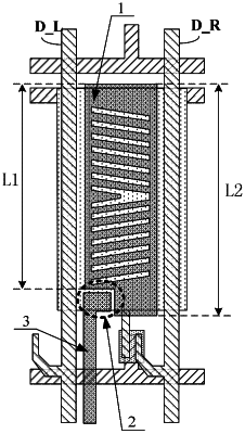
the plurality of gate lines and the plurality of data lines define a plurality of pixel units, each of the pixel units comprises a thin film transistor, a pixel electrode and a common electrode, the pixel electrode is on a side of the common electrode distal to the first substrate; in a same pixel unit, a region where the pixel electrode is located and a region where the thin film transistor is located are arranged in the second direction, an end of the pixel electrode proximal to the thin film transistor is a first end, an end of the pixel electrode distal to the thin film transistor is a second end; at least some of the pixel units are configured with conductive bridge lines, respectively, the conductive bridge lines are provided in the same layer as the pixel electrode;
in the pixel unit which is configured with the conductive bridge line, a first hollowed-out structure is provided on a first side of the first end or the second end of the pixel electrode, an end of the conductive bridge line is located in the first hollowed-out structure and is connected to the common electrode through a via, and a second hollowed-out structure is provided on a second side of the second end of the pixel electrode, so that an absolute value of a difference between parasitic capacitances formed respectively by the pixel electrode and nearest data lines located on both sides of the pixel electrode is less than or equal to a preset capacitance difference;
the first side and the second side are opposite sides of the pixel electrode in the first direction;
wherein, for any one of the pixel units, a polarity of a data voltage applied to a nearest data line on a side of the pixel electrode is inverted, and an amount of change in a voltage applied to the pixel electrode in the pixel unit due to the polarity inversion is ΔVp:
ΔVp=Cpd1*ΔVd/(Cpd1+Cpd2+Cst+Clc+Cgp)
where Cpd1 represents a parasitic capacitance formed between the pixel electrode in the pixel unit and the data line where the polarity inversion occurs, ΔVd represents a difference between the data voltage applied after the polarity inversion and the data voltage applied before the polarity inversion on the data line where the polarity inversion occurs, Cpd1+Cpd2 represents a sum of parasitic capacitances formed respectively between the pixel electrode in the pixel unit and nearest data lines located on both sides of the pixel electrode, Cst represents a storage capacitance between the pixel electrode in the pixel unit and the common electrode, Clc represents a liquid crystal capacitance at the pixel unit, and Cgp represents a parasitic capacitance between the pixel electrode in the pixel unit and the gate line;
wherein the opposite substrate is a color filter substrate which comprises: a second base substrate, and color filter patterns and a black matrix which are located on the second base substrate;
the black matrix defines multiple pixel light outgoing openings being in one-to-one correspondence with the pixel units, and the color filter patterns are located in the pixel light outgoing openings, respectively; and
an orthogonal projection of the black matrix on the first base substrate completely covers orthogonal projections of the gate lines, the data lines, the thin film transistor, the first hollowed-out structure and the second hollowed-out structure on the first base substrate.
|