| CPC G09G 3/3266 (2013.01) [G09G 3/2096 (2013.01); G09G 3/3233 (2013.01); G09G 2300/0426 (2013.01); G09G 2300/0819 (2013.01); G09G 2300/0842 (2013.01); G09G 2310/0202 (2013.01); G09G 2310/0291 (2013.01); G09G 2310/08 (2013.01); G09G 2360/14 (2013.01); G09G 2380/08 (2013.01)] | 13 Claims |
|
1. A display device, comprising:
a display panel comprising scan write lines, sensing lines, pixels respectively connected to the scan write lines, and optical sensors respectively connected to the scan write lines and the sensing lines;
a scan driver configured to sequentially output scan write signals to the scan write lines in response to a scan control signal;
a read-out circuit configured to receive light sensing signals of the optical sensors from the sensing lines in response to a first sampling signal; and
a timing controller configured to control the scan driver and the read-out circuit,
wherein an interval between pulses of the first sampling signal has a first horizontal period, and an interval between pulses of each of the scan write signals has a second horizontal period,
wherein each of the optical sensors comprises:
a photoelectric conversion element comprising an anode electrode and a cathode electrode connected to a voltage line;
a first sensing transistor comprising a gate electrode connected to the anode electrode of the photoelectric conversion element,
a reset transistor configured to connect a reset voltage line to the anode electrode of the photoelectric conversion element in response to a reset signal; and
a second sensing transistor configured to connect the first sensing; transistor to a corresponding one of the sensing lines in response to the scan write signal input thereto,
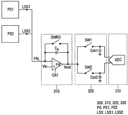
wherein the read-out circuit comprises:
an amplifier connected to the corresponding one of the sensing lines and comprising an operational amplifier,
a sampling unit comprising a first sampling capacitor configured to hold a voltage of one of the light sensing signals in response to the first sampling signal; and
an analog-digital (AD) converter configured to convert the held light sensing signal voltage into digital data,
wherein each of the second sensing transistors is turned on in response to a corresponding one of the scan write signals to output a sensing signal voltage through the sensing line to which it is connected, and
each of the sensing signal voltages is held in the first sampling capacitor in response to the first sampling signal,
wherein the first sampling signal has a first period in which the first sampling capacitor is turned on and a second period in which the first sampling capacitor is turned off,
wherein in the first period, the first sampling capacitor accumulates and holds at least two sensing signal voltages among the sensing signal voltages, the at least two sensing signal voltages including a first sensing signal voltage output from a first optical sensor connected to a first scan write line and a second sensing signal voltage output from a second optical sensor connected to a second scan write line.
|