| CPC G09G 3/3266 (2013.01) [G09G 3/2092 (2013.01); G11C 19/28 (2013.01); G09G 2300/0852 (2013.01); G09G 2310/0267 (2013.01); G09G 2310/0275 (2013.01); G09G 2310/0291 (2013.01); G09G 2310/08 (2013.01)] | 20 Claims |

|
1. A gate driving circuit comprising:
a plurality of stage circuits dependently connected to each other, each of the plurality of stage circuits being configured to output ‘j’ output signals, ‘j’ being an integer greater than or equal to 2,
wherein each of the plurality of stage circuits includes:
a logic controller for controlling a first voltage of a first node and a second voltage of a second node; and
an output circuit for outputting each of ‘j’ clock signals as a respective output signal of the ‘j’ output signals in response to the first voltage of the first node,
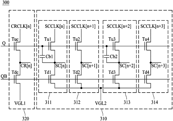
wherein the output circuit includes:
‘j’ output buffers, each of the ‘j’ output buffers being for outputting a respective clock signal of the ‘j’ clock signals as one of the ‘j’ output signals through a respective output node in response to the first voltage of the first node; and
a plurality of capacitors connected between the first node and the respective output node of some of the ‘j’ output buffers,
wherein the ‘j’ clock signals include first to (j)th scan clock signals,
the first to (j)th scan clock signals are sequentially shifted, each scan clock signal of the first to (j)th scan clock signals has the first voltage level for a first period, and adjacent scan clock signals of the first to (j)th scan clock signals overlap each other for a second period shorter than the first period, and
the ‘j’ output buffers include first to (j)th scan signal output buffers respectively applied with the first to (j)th scan clock signals.
|