| CPC G09G 3/3233 (2013.01) [G09G 2300/0819 (2013.01); G09G 2300/0842 (2013.01); G09G 2310/08 (2013.01)] | 19 Claims |

|
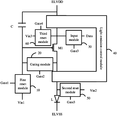
1. A pixel circuit, wherein the pixel circuit is configured to drive, in an Xth frame period, a light emitting device electrically connected to the pixel circuit to emit light; the Xth frame period comprises Y data writing stages and Z light emitting stages, a yth data writing stage in the Y data writing stages comprises a first sub-stage, a second sub-stage and a third sub-stage, and the pixel circuit comprises:
a driving transistor;
a first reset module electrically connected to the driving transistor, wherein the first reset module is configured to transmit, in the first sub-stage, a first initialization signal to the driving transistor in response to a first scanning signal;
a gating module electrically connected to the driving transistor, wherein the gating module is configured to perform, in the second sub-stage, a threshold compensation on the driving transistor in response to a second scanning signal; and
an input module electrically connected to the driving transistor, wherein the input module is configured to transmit, in the third sub-stage, a data signal to the driving transistor in response to a third scanning signal;
wherein X, Y, Z and y are positive integers, y is less than or equal to Y, and Y is greater than Z;
wherein the Xth frame period further comprises a plurality of reset stages, and each data writing stage follows at least one reset stage; and
wherein the pixel circuit further comprises a third reset module, the third reset module is electrically connected to a fourth scanning terminal, a third initialization terminal and a second electrode of the driving transistor, and the third reset module is configured to: transmit, in the reset stage, a third initialization signal of the third initialization terminal to the second electrode of the driving transistor in response to a fourth scanning signal of the fourth scanning terminal.
|