| CPC G09G 3/3233 (2013.01) [G02F 1/133553 (2013.01); G02F 1/1368 (2013.01); G09G 3/035 (2020.08); G09G 3/3648 (2013.01); G09G 5/10 (2013.01); H10K 59/00 (2023.02); H10K 59/128 (2023.02); H10K 59/50 (2023.02); H10K 77/111 (2023.02); G02F 1/133305 (2013.01); G02F 1/133512 (2013.01); G02F 1/133514 (2013.01); G02F 1/133565 (2021.01); G02F 1/136227 (2013.01); G02F 1/13685 (2021.01); G02F 2201/44 (2013.01); G09G 3/3666 (2013.01); G09G 3/3696 (2013.01); G09G 2300/023 (2013.01); G09G 2320/0233 (2013.01); G09G 2320/045 (2013.01); G09G 2330/12 (2013.01); G09G 2380/02 (2013.01); H01L 27/1225 (2013.01); H01L 29/7869 (2013.01); H10K 59/1213 (2023.02); H10K 59/124 (2023.02); H10K 59/38 (2023.02); H10K 2102/311 (2023.02)] | 13 Claims |
|
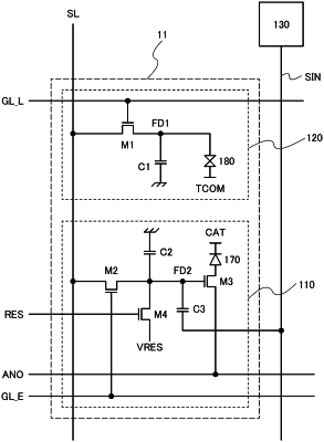
1. An information terminal comprising a display portion,
wherein the display portion includes a first pixel, a second pixel, a sensor element, a first gate line, a second gate line, and a source line,
wherein the first pixel comprises a first transistor and a liquid crystal element,
wherein the second pixel comprises a second transistor, a third transistor, a capacitor, and a light-emitting element,
wherein a gate of the first transistor is electrically connected to the first gate line, one of a source and a drain of the first transistor is electrically connected to the source line, and the other of the source and the drain of the first transistor is electrically connected to the liquid crystal element,
wherein a gate of the second transistor is electrically connected to the second gate line, one of a source and a drain of the second transistor is electrically connected to the source line, and the other of the source and the drain of the second transistor is electrically connected to a gate of the third transistor,
wherein the gate of the third transistor is electrically connected to the sensor element through the capacitor and one of a source and a drain of the third transistor is electrically connected to the light-emitting element,
wherein the sensor element includes a first bend sensor whose resistance is changed in accordance with bending of the display portion in a convex direction and a second bend sensor whose resistance is changed in accordance with bending of the display portion in a concave direction, and
wherein a luminance of the light-emitting element is controlled in accordance with an output of the sensor element.
|