| CPC G09F 9/3026 (2013.01) [G09F 9/33 (2013.01); H01L 27/156 (2013.01); H01L 33/62 (2013.01)] | 20 Claims |
|
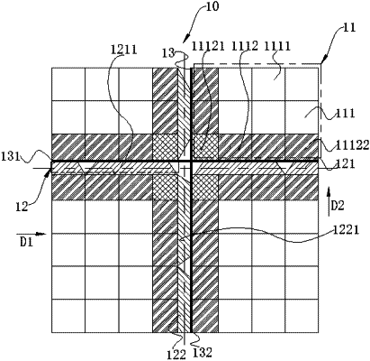
1. A light emitting diode (LED) splicing display panel, comprising at least one repeat unit, wherein each of the repeat unit comprises four sub-LED display panels spliced to each other, a plurality of display regions of the four sub-LED display panels are arranged in two rows and two columns, each of the sub-LED display panels comprises a corresponding display region of the plurality of display regions and a plurality of fan-out regions disposed at two adjacent sides of the corresponding display region, a plurality of slits are between two adjacent sub-LED display panels, and the two adjacent sub-LED display panels share the plurality of fan-out regions;
wherein a plurality of sub-pixels are in the plurality of display regions, the plurality of sub-pixels comprise a plurality of irregular-shaped sub-pixels located on edges of the plurality of display regions, and a plurality of regular-shaped sub-pixels respectively adjacent to the plurality of irregular-shaped sub-pixels, each of the plurality of irregular-shaped sub-pixels abuts to a corresponding fan-out region, and a display area of each of the plurality of irregular-shaped sub-pixels is less than a display area of each of the regular-shaped sub-pixels.
|