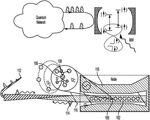
| CPC G06N 10/70 (2022.01) [B82Y 20/00 (2013.01); G02B 6/1225 (2013.01)] | 20 Claims |

|
1. A method of making a quantum network node comprising:
calculating a plurality of scoring function F values for an array of at least two photonic crystal cavity unit cells, each photonic crystal cavity unit cell having a lattice constant α and a hole having a length Hx and a width Hy, wherein the scoring function comprises:
F=min(Q,Qcutoff)/(Qcutoff×Vmode)
wherein Q is a cavity quality factor, Qcutoff is an estimated maximum realizable Q, and Vmode is a cavity mode volume;
selecting a value of α, a value of Hx, and a value of Hy for which the scoring function value meets a scoring function value criteria;
forming, on a substrate, a waveguide region and the array of at least two photonic crystal cavity unit cells based on the selected value a, the selected value Hz, and the selected value Hy;
implanting at least one ion between a hole of a first photonic crystal cavity unit cell and a second photonic crystal cavity unit cell;
annealing the at least one implanted ion into at least one quantum defect; and
forming a coplanar microwave waveguide on the substrate configured to be electromagnetically coupled to the array of at least two photonic crystal cavity unit cells.
|