| CPC G06F 9/3001 (2013.01) [G06F 9/3004 (2013.01); G11C 11/4023 (2013.01); G11C 11/4085 (2013.01); G11C 11/4093 (2013.01); G11C 11/4094 (2013.01)] | 3 Claims |
|
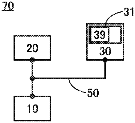
1. A memory device comprising:
a plurality of memory cells including a first memory region and a second memory region,
wherein, when the memory device is activated, the second memory region includes a first space in which binary data are stored, a second space in which multilevel data are stored, and a free space,
wherein the first memory region is a volatile memory,
wherein the first memory region is a first main memory device,
wherein the free space is configured to be used as a second main memory device,
wherein the first memory region and the free space are configured to be used when an arithmetic processing is performed, and
wherein the second main memory device is a nonvolatile memory.
|