| CPC G06F 3/0445 (2019.05) [G06F 3/047 (2013.01)] | 5 Claims |

|
1. A display device comprising:
a display panel; and
a touch panel on the display panel, the touch panel comprising:
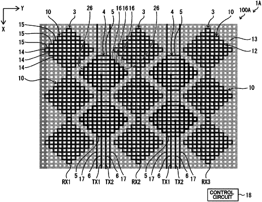
a plurality of detection electrodes extending in a first direction in a plan view; and
a plurality of drive electrodes disposed respectively between the plurality of detection electrodes and extending in the first direction, each of the plurality of drive electrodes comprising:
a plurality of electrode segments patterned in the first direction; and
a plurality of wires connected respectively to one of the plurality of electrode segments and extending in the first direction,
wherein
the touch panel further comprises:
a first electrode layer;
a second electrode layer between the first electrode layer and the display panel; and
an insulation layer between the first electrode layer and the second electrode layer,
the plurality of detection electrodes and the plurality of electrode segments of the plurality of drive electrodes are provided in the first electrode layer,
the plurality of wires of the plurality of drive electrodes are provided in the second electrode layer, and
at least one of the plurality of wires overlaps, and is not connected to, another electrode segment being different from the one of the plurality of electrode segments in the first direction.
|