| CPC G06F 3/0412 (2013.01) [G02F 1/13338 (2013.01); G02F 1/133512 (2013.01); G02F 1/133528 (2013.01); G02F 2202/28 (2013.01); G06F 3/0446 (2019.05); G06F 2203/04107 (2013.01)] | 8 Claims |
|
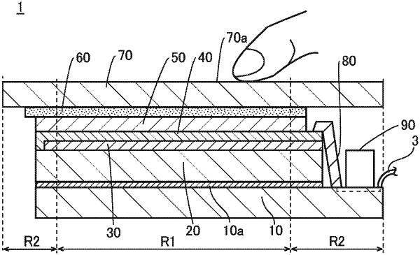
1. An in-cell touch panel having a touch surface that is touched by an indicator, the in-cell touch panel comprising:
a touch electrode;
a shielding layer that is conductive and that is disposed between the touch electrode and the touch surface;
a conductive layer that is electrically connected to the shielding layer; and
wiring that connects the conductive layer to a reference potential, wherein
the touch surface has
a touch detection region that, when touched by the indicator, detects the touch by the touch electrode, and
a frame region that is disposed on an outer side of the touch detection region,
at least part of the shielding layer is disposed so as to overlap the touch detection region in plan view,
at least part of the conductive layer is disposed so as to overlap the frame region in plan view, and
a sheet resistance value of the conductive layer is lower than a sheet resistance value of the shielding layer.
|