| CPC G06F 13/28 (2013.01) [G06F 2213/28 (2013.01)] | 20 Claims |
|
1. A method for an embedded processor in a System on a Chip (SoC) to perform fast data communication, wherein the method comprises:
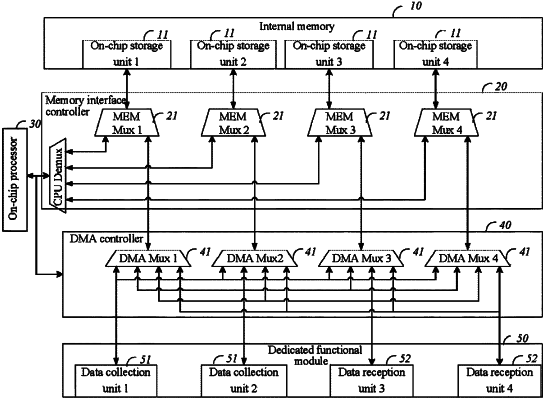
dividing an internal memory into multiple on-chip storage units which are sequentially assigned with consecutive addresses, wherein read or write operations between different on-chip storage units are independent of each other and are able to be performed simultaneously;
enabling a memory interface controller connected to the internal memory, the memory interface controller comprising multiple memory interface control units, wherein each memory interface control unit corresponds to at least one on-chip storage unit, and each on-chip storage unit uniquely corresponds to one memory interface control unit;
enabling an on-chip processor and a Direct Memory Access (DMA) controller which are respectively connected to the memory interface controller, the DMA controller comprising multiple request allocation units in one-to-one correspondence with the memory interface control units, wherein an address corresponding to request information processed by each request allocation unit matches an address range of the on-chip processor, and the address corresponding to the request information processed by each request allocation unit matches an address of the on-chip storage unit corresponding to the respective request allocation unit;
enabling a dedicated functional module connected to the DMA controller, the dedicated functional module comprising multiple data collection units and multiple data reception units, wherein the on-chip processor is adapted to configure an address range of the internal memory corresponding to each of the multiple data collection units and the multiple data reception units, and each data collection unit and data reception unit in the dedicated functional module is connected to each of the multiple request allocation units; and
when the on-chip processor executes a read or write request on the internal memory, the memory interface control unit determining a corresponding on-chip storage unit according to an address carried in the request information of the read or write request and sending the read or write request to the determined corresponding on-chip storage unit, so as to read or write data in the internal memory, and when data is read from the internal memory, returning the read data to an original request module; and when the dedicated functional module executes a read or write request on the internal memory through the DMA controller, the DMA controller sending the read or write request through the corresponding request allocation unit to the corresponding memory interface control unit according to an address carried in the request information of the read or write request, and the corresponding memory interface control unit determining a corresponding on-chip storage unit according to the address carried in the request information of the read or write request and sending the read or write request to the determined corresponding on-chip storage unit, so as to read or write data in the internal memory, and when data is read from the internal memory, returning the read data to an original request module.
|