| CPC G06F 11/1068 (2013.01) [G06F 3/0604 (2013.01); G06F 3/0659 (2013.01); G06F 3/0679 (2013.01); G11C 29/52 (2013.01); G06F 3/065 (2013.01); G11B 2020/1823 (2013.01); G11C 7/1006 (2013.01); G11C 11/5628 (2013.01); G11C 13/0069 (2013.01); G11C 16/10 (2013.01); G11C 29/42 (2013.01); G11C 2211/5646 (2013.01); G11C 2211/5647 (2013.01)] | 20 Claims |

|
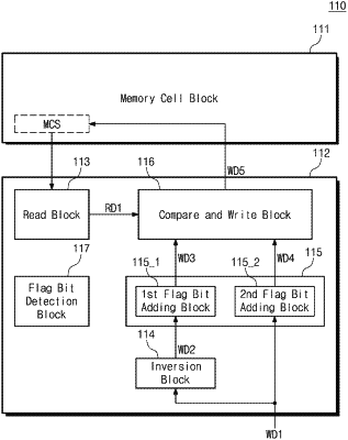
13. A nonvolatile memory device comprising:
a plurality of memory cells;
an inversion circuit configured to receive first write data, and to invert the first write data to generate second write data;
a flag bit adding circuit configured to receive the first write data and the second write data, to add a first flag bit to the second write data to generate third write data including the first flag bit, and to add a second flag bit to the first write data to generate fourth write data including the second flag bit; and
a compare and write circuit configured to receive the third write data including the first flag bit and the fourth write data including the second flag bit, to perform a first comparison between a first read data and the third write data including the first flag bit, to perform a second comparison between the first read data and the fourth write data including the second flag bit, to select one of the third write data including the first flag bit and the fourth write data including the second flag bit based on a result of the first comparison and the second comparison, and to write the selected one of the third write data including the first flag bit and the fourth write data including the second flag bit in the plurality of memory cells,
wherein both the first comparison and the second comparison occur after the flag bit adding circuit outputs both the third write data including the first flag bit and the fourth write data including the second flag bit to the compare and write circuit.
|