| CPC G05F 3/262 (2013.01) [G01K 7/01 (2013.01); H03M 1/34 (2013.01); H03M 3/458 (2013.01); G01K 2217/00 (2013.01); H02M 3/07 (2013.01)] | 20 Claims |
|
1. An apparatus, comprising:
a functional circuit block coupled to a global power supply node;
a power converter circuit configured to generate a regulated voltage level on a local power supply node using the regulated voltage level of the global power supply node, wherein the regulated voltage level is greater than a voltage level of an input power supply node, wherein the power converter circuit includes:
a passgate having a first terminal coupled to receive the voltage level of the global power supply node;
a ring oscillator configured to generate a periodic signal; and
a feedback circuit coupled between the local power supply node and the passgate and configured to sample the regulated voltage level in accordance with the periodic signal and further configured to control the passgate based on samples of the regulated voltage level;
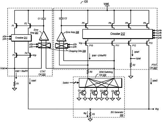
a sensor circuit coupled to the local power supply node, wherein the sensor circuit includes switching circuitry, a first plurality of devices and a second plurality of devices, wherein the switching circuitry is configured to, at different ones of a plurality of time points, randomly select ones of the first plurality of devices to form first and second subsets, and further configured to at the different ones of the plurality of time points, couple ones of the first and second subsets to first and second circuit branches, respectively, the first and second circuit branches including ones of the second plurality of devices, and wherein the sensor circuit is further configured to:
compare corresponding parameters of different ones of the first and second subsets of the first plurality of devices selected by the switching circuitry at a particular one of the plurality of time points to generate a plurality of comparison results; and
generate an analog signal using the plurality of comparison results, wherein the analog signal is proportional to an operating parameter associated with the functional circuit block; and
an analog-to-digital converter (ADC) circuit coupled to the local power supply node, wherein the analog-to-digital converter circuit is configured to generate a plurality of bits using the analog signal.
|