| CPC G03F 1/26 (2013.01) [G03F 1/50 (2013.01); G03F 1/54 (2013.01); G03F 7/20 (2013.01)] | 18 Claims |
|
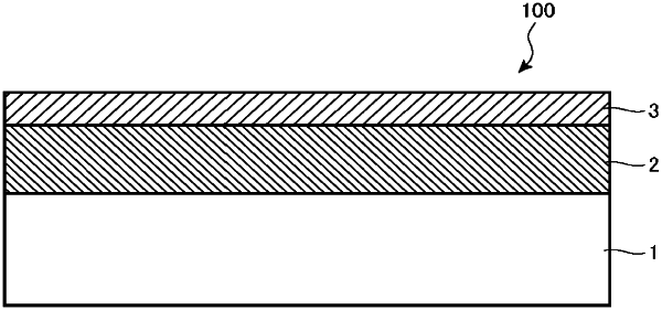
1. A mask blank comprising:
a transparent substrate; and
a light shielding film on the transparent substrate,
wherein the light shielding film includes:
a lower layer on the transparent substrate; and
an upper layer on the lower layer,
wherein the lower layer contains silicon and nitrogen,
wherein the upper layer contains silicon and oxygen,
wherein an optical density to an ArF excimer laser exposure light of the light shielding film is 2.5 or more,
wherein a surface reflectance to the exposure light of the light shielding film is 30% or less,
wherein a back-surface reflectance to the exposure light of the light shielding film is 40% or less,
wherein a transmittance to a light having a wavelength of 900 nm of the light shielding film is 50% or less,
wherein an extinction coefficient k to a light having a wavelength of 900 nm of the light shielding film is 0.04 or more, and
wherein a thickness of the light shielding film is 60 nm or less.
|