| CPC G02F 1/163 (2013.01) [G02F 1/155 (2013.01); G02F 1/157 (2013.01); G02F 2001/1552 (2013.01)] | 20 Claims |

|
1. An electrochromic device obtained by production process, comprising:
providing a substrate and a stack overlying the substrate, the stack comprising:
a first transparent conductive layer over the substrate;
a second transparent conductive layer over the substrate;
a cathodic electrochemical layer between the first transparent conductive layer and the second transparent conductive layer; and
an anodic electrochemical layer between the first transparent conductive layer and the second transparent conductive layer; and
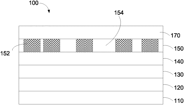
patterning a first region of the second transparent conductive layer without removing the material from the first region, wherein after patterning the first region, the first region comprises a first resistivity and a second region of the second transparent conductive layer comprises a second resistivity, wherein the first resistivity is different from the second resistivity, wherein patterning the second transparent conductive layer to form the first resistivity and the second resistivity is patterned through an insulating layer; wherein the first region and the second region comprise the same material.
|