| CPC G02F 1/136286 (2013.01) [G02F 1/133528 (2013.01); G09G 3/20 (2013.01); G09G 3/3233 (2013.01); G09G 3/3677 (2013.01); G11C 19/28 (2013.01); H10K 10/482 (2023.02); G02F 1/133638 (2021.01); G09G 2300/0408 (2013.01); G09G 2300/0417 (2013.01); G09G 2300/0847 (2013.01); G09G 2310/0254 (2013.01); G09G 2310/0267 (2013.01); G09G 2310/0286 (2013.01); G09G 2310/0291 (2013.01); G09G 2310/08 (2013.01); G09G 2320/043 (2013.01); H10K 10/20 (2023.02)] | 8 Claims |

|
1. A semiconductor device comprising:
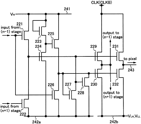
a first circuit comprising a first transistor, a second transistor, a third transistor, a fourth transistor, a fifth transistor, a sixth transistor, a seventh transistor, an eighth transistor, a ninth transistor, a tenth transistor, and an eleventh transistor;
a second circuit in a previous stage of the first circuit; and
a third circuit in a subsequent stage of the first circuit,
wherein one of a source and a drain of the first transistor is electrically connected to a first wiring,
wherein a clock signal is input to the first wiring,
wherein the other of the source and the drain of the first transistor is electrically connected to one of a source and a drain of the second transistor, the second circuit, and the third circuit,
wherein one of a source and a drain of the third transistor and one of a source and a drain of the eighth transistor are electrically connected to a pixel,
wherein the other of the source and the drain of the third transistor is electrically connected to a fourth wiring,
wherein one of a source and a drain of the fifth transistor and one of a source and a drain of the sixth transistor are electrically connected to a third wiring,
wherein a gate of the second transistor is electrically connected to a gate of the fifth transistor, the other of the source and the drain of the sixth transistor, and one of a source and a drain of the ninth transistor,
wherein a gate of the seventh transistor is electrically connected to a fifth wiring,
wherein a first signal is input to the fifth wiring from the third circuit,
wherein a gate of the fourth transistor is electrically connected to a second wiring,
wherein a second signal is input to the second wiring from the second circuit,
wherein one of a source and a drain of the fourth transistor is electrically connected to the other of the source and the drain of the fifth transistor, one of a source and a drain of the seventh transistor, and a gate of the first transistor,
wherein a gate of the ninth transistor is directly connected to one of a source and a drain of the tenth transistor, and
wherein the gate of the ninth transistor is directly connected to one of a source and a drain of the eleventh transistor.
|