| CPC G01S 7/4816 (2013.01) [G01S 17/08 (2013.01); H01L 27/14607 (2013.01); H01L 27/14614 (2013.01); H01L 27/14645 (2013.01); H01L 27/14649 (2013.01); H04N 23/11 (2023.01); H04N 25/77 (2023.01); H04N 25/79 (2023.01)] | 26 Claims |
|
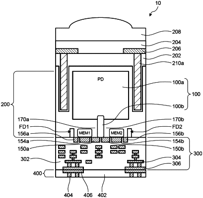
1. A light receiving device comprising a light receiving unit that includes a plurality of light receiving elements arranged in a row direction and a column direction on a semiconductor substrate, wherein
each of the light receiving elements includes:
a first photoelectric conversion unit that converts light into electric charges;
a first electric charge storage unit to which the electric charges are transferred from the first photoelectric conversion unit;
a first distribution gate that distributes the electric charges from the first photoelectric conversion unit to the first electric charge storage unit;
a second electric charge storage unit to which the electric charges are transferred from the first photoelectric conversion unit; and
a second distribution gate that distributes the electric charges from the first photoelectric conversion unit to the second electric charge storage unit, and
the first and second distribution gates are provided at positions axially symmetric to each other with respect to a first center axis extending so as to pass through the center of the first photoelectric conversion unit, in a direction intersecting the column direction at a predetermined angle, when viewed from above the semiconductor substrate,
wherein each of the light receiving elements further includes first and second discharge gates that discharge the electric charges in the first photoelectric conversion unit, and
the first and second discharge gates are provided at positions axially symmetric to each other with respect to a second center axis orthogonal to the first center axis so as to pass through the center of the first photoelectric conversion unit, when viewed from above the semiconductor substrate.
|