US 12,012,473 B2
Directed self-assembly structures and techniques
James Munro Blackwell, Portland, OR (US); Robert L. Bristol, Portland, OR (US); Xuanxuan Chen, Hillsboro, OR (US); Lauren Elizabeth Doyle, Portland, OR (US); Florian Gstrein, Portland, OR (US); Eungnak Han, Portland, OR (US); Brandon Jay Holybee, Portland, OR (US); Marie Krysak, Portland, OR (US); Tayseer Mahdi, Beaverton, OR (US); Richard E. Schenker, Portland, OR (US); Gurpreet Singh, Portland, OR (US); and Emily Susan Walker, Hillsboro, OR (US)
Assigned to Intel Corporation, Santa Clara, CA (US)
Filed by Intel Corporation, Santa Clara, CA (US)
Filed on Sep. 25, 2020, as Appl. No. 17/032,517.
Claims priority of provisional application 63/033,721, filed on Jun. 2, 2020.
Prior Publication US 2021/0375745 A1, Dec. 2, 2021
Int. Cl. G03F 7/11 (2006.01); C08F 265/02 (2006.01); C08F 265/04 (2006.01); H01L 23/522 (2006.01); H01L 23/528 (2006.01)
CPC C08F 265/04 (2013.01) [C08F 265/02 (2013.01); G03F 7/11 (2013.01); H01L 23/5226 (2013.01); H01L 23/528 (2013.01)] 20 Claims
OG exemplary drawing
 
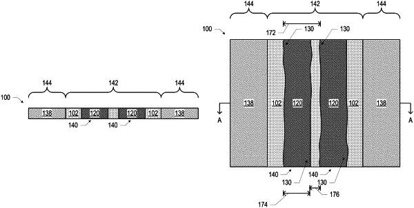
1. A microelectronic structure, comprising:
a patterned region including a first conductive line and a second conductive line, wherein the first conductive line and the second conductive line have a pitch that is less than 30 nanometers, the first conductive line has a line edge roughness that is less than 1.2 nanometers, and the second conductive line has a line edge roughness that is less than 1.2 nanometers; and
an unpatterned region having an unordered lamellar pattern, wherein the unpatterned region is adjacent to the patterned region.