US 12,011,784 B2
Wafer, wafer manufacturing method, device chip manufacturing method, and resistivity markings
Kazuma Sekiya, Tokyo (JP)
Assigned to DISCO CORPORATION, Tokyo (JP)
Filed by DISCO CORPORATION, Tokyo (JP)
Filed on Jul. 22, 2021, as Appl. No. 17/382,921.
Claims priority of application No. 2020-131713 (JP), filed on Aug. 3, 2020.
Prior Publication US 2022/0032404 A1, Feb. 3, 2022
Int. Cl. B23K 26/53 (2014.01); B23K 26/40 (2014.01); B23K 103/00 (2006.01); H01L 21/78 (2006.01)
CPC B23K 26/53 (2015.10) [B23K 26/40 (2013.01); H01L 21/78 (2013.01); B23K 2103/56 (2018.08)] 7 Claims
OG exemplary drawing
 
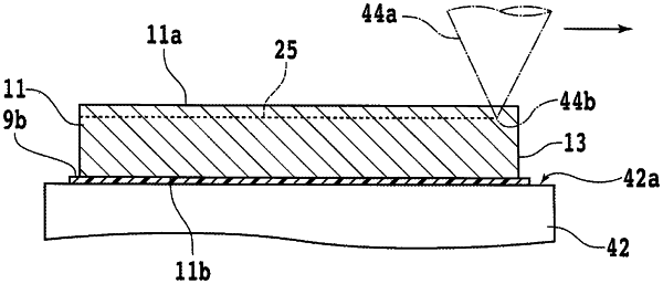
1. A wafer wherein a character, a number, or a mark representing information regarding resistivity is formed at a predetermined height position inside the wafer along a curved portion of an outer periphery of the wafer; and
wherein the character, the number, or the mark representing information regarding resistivity is formed along the entire outer periphery of the wafer.