| CPC H10N 70/8418 (2023.02) [H01L 21/28562 (2013.01); H01L 21/28568 (2013.01); H01L 21/31053 (2013.01); H01L 21/31144 (2013.01); H01L 21/3212 (2013.01); H01L 21/76879 (2013.01); H10B 63/80 (2023.02); H10N 70/021 (2023.02); H10N 70/063 (2023.02); H10N 70/231 (2023.02); H10N 70/826 (2023.02); H10N 70/8413 (2023.02); H10N 70/8828 (2023.02); H10N 70/8833 (2023.02)] | 20 Claims |
|
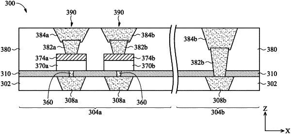
1. A method comprising:
forming a first dielectric layer over a first electrode layer;
forming a patterned second dielectric layer over the first dielectric layer;
forming a sacrificial layer on the patterned second dielectric layer;
forming a trench through the sacrificial layer that exposes the first electrode layer;
forming a conductive material in the trench; and
after forming the conductive material in the trench, removing at least a first portion of the sacrificial layer and at least a first portion of the patterned second dielectric layer to expose a portion of the first dielectric layer.
|