US 12,010,929 B2
Memory device and manufacturing method therefor
Tae Joo Park, Ansan-si (KR); Dae Woong Kim, Ansan-si (KR); Tae Jun Seok, Yongin-si (KR); and Hye Rim Kim, Dongducheon-si (KR)
Assigned to INDUSTRY-UNIVERSITY COOPERATION FOUNDATION HANYANG UNIVERSITY ERICA CAMPUS, Ansan-Si (KR)
Filed by INDUSTRY-UNIVERSITY COOPERATION FOUNDATION HANYANG UNIVERSITY ERICA CAMPUS, Ansan-Si (KR)
Filed on May 11, 2021, as Appl. No. 17/316,794.
Application 17/316,794 is a continuation in part of application No. PCT/KR2019/018519, filed on Dec. 26, 2019.
Claims priority of application No. 10-2018-0169696 (KR), filed on Dec. 26, 2018.
Prior Publication US 2021/0273158 A1, Sep. 2, 2021
Int. Cl. H01L 45/00 (2006.01); C23C 16/40 (2006.01); C23C 16/455 (2006.01); C23C 16/52 (2006.01); G11C 13/00 (2006.01); H10N 70/00 (2023.01); H10N 70/20 (2023.01)
CPC H10N 70/245 (2023.02) [C23C 16/40 (2013.01); C23C 16/403 (2013.01); C23C 16/45529 (2013.01); C23C 16/45553 (2013.01); C23C 16/52 (2013.01); G11C 13/0011 (2013.01); G11C 13/0069 (2013.01); H10N 70/023 (2023.02); H10N 70/826 (2023.02); H10N 70/8836 (2023.02)] 18 Claims
OG exemplary drawing
 
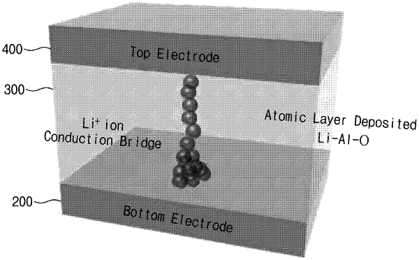
1. A memory device comprising:
a first electrode;
a resistance change layer disposed on the first electrode and including lithium, aluminum, and oxygen; and
a second electrode disposed on the resistance change layer,
wherein the resistance change layer has a lithium content ratio Li/(Li+Al) that is more than 40 at % and less than 60 at %.