| CPC H10K 77/111 (2023.02) [H10K 50/844 (2023.02); H10K 59/12 (2023.02); G02F 1/133305 (2013.01); G06F 1/1641 (2013.01); G06F 1/1652 (2013.01); G09F 9/301 (2013.01); G09G 3/035 (2020.08); G09G 3/3233 (2013.01); G09G 2300/0809 (2013.01); H10K 50/818 (2023.02); H10K 50/828 (2023.02); H10K 59/121 (2023.02); H10K 59/1216 (2023.02); H10K 59/122 (2023.02); H10K 59/351 (2023.02); H10K 2102/311 (2023.02)] | 23 Claims |
|
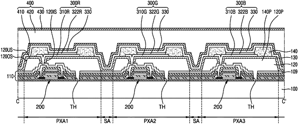
1. A display device comprising:
a flexible substrate;
a pixel circuit layer arranged on the flexible substrate, comprising a thin-film transistor, and defining a through hole extending to the flexible substrate;
a first organic layer arranged on the pixel circuit layer, in contact with the flexible substrate through the through hole, and defining a first opening above the thin-film transistor and exposing at least a portion of an upper surface of the pixel circuit layer;
an inorganic layer arranged on the first organic layer to cover an upper surface of the first organic layer, and to cover sidewalls of the first organic layer that define the first opening;
a pixel electrode arranged on the inorganic layer; and
an encapsulation layer arranged on the pixel electrode, and comprising a first inorganic encapsulation layer, a second inorganic encapsulation layer, and an organic encapsulation layer between the first inorganic encapsulation layer and the second inorganic encapsulation layer.
|