| CPC H10K 77/10 (2023.02) [H10K 50/8426 (2023.02); H10K 50/8445 (2023.02); H10K 59/12 (2023.02); H10K 59/124 (2023.02); H10K 71/231 (2023.02); H01L 27/1237 (2013.01); H10K 59/1201 (2023.02); Y02E 10/549 (2013.01); Y02P 70/50 (2015.11)] | 38 Claims |
|
1. A display apparatus, comprising:
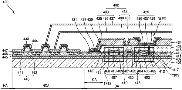
a substrate including a front surface and a rear surface, the substrate having a hole that passes from the front surface to the rear surface;
a plurality of light-emitting elements on the front surface of the substrate and defining a display area around the hole, each of the plurality of light-emitting elements being electrically connected to a transistor and a capacitor;
two dams spaced apart from each other in a non-display area of the substrate and disposed between the hole and the display area, each of the two dams extending along an edge of the hole of the substrate to entirely surround the hole of the substrate in a plan view;
an encapsulation layer over the plurality of light-emitting elements and comprising a first inorganic layer, a second inorganic layer, and an organic layer between the first inorganic layer and the second inorganic layer; and
a plurality of metal layers, in the non-display area, arranged between the two dams and the hole of the substrate.
|