| CPC H10K 59/65 (2023.02) [H10K 50/865 (2023.02); H10K 71/00 (2023.02)] | 10 Claims |
|
1. A display device, comprising: an imaging area and a display area on at least one side of the imaging area;
the imaging area comprising:
a substrate;
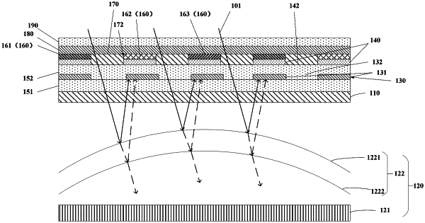
an image collection device on a side of the substrate, the image collection device comprising a photosensitive element and an optical element between the photosensitive element and the substrate;
a light blocking layer on a side of the substrate away from the image collection device, wherein the light blocking layer comprises at least one of a light absorbing layer or a diffuse reflection layer, and the light blocking layer is provided with a first gap; and
a plurality of first electrodes on a side of the light blocking layer away from the substrate, wherein a second gap is provided between two adjacent first electrodes of the plurality of first electrodes, and each of the plurality of first electrodes is electrically connected to a pixel driving circuit located in the display area through a connection;
wherein an orthographic projection of the light blocking layer on the substrate at least partially overlaps with an orthographic projection of the plurality of first electrodes on the substrate, and an orthographic projection of the first gap on the substrate at least partially overlaps with an orthographic projection of the second gap on the substrate;
wherein the imaging area further comprises:
a functional layer on a side of each of the plurality of first electrodes away from the substrate, the functional layer comprising a light emitting layer;
a second electrode on a side of the functional layer away from the plurality of first electrodes; and
an encapsulation layer on a side of the second electrode away from the functional layer.
|