| CPC H10K 59/65 (2023.02) [G06V 40/1318 (2022.01); H10K 59/1201 (2023.02); H10K 59/122 (2023.02); H10K 59/38 (2023.02); H10K 59/873 (2023.02); H10K 59/8792 (2023.02); H10K 77/111 (2023.02); H10K 2102/311 (2023.02)] | 16 Claims |
|
1. An organic light-emitting diode (OLED) display device, comprising:
a flexible substrate;
a thin film transistor (TFT) array layer disposed on the flexible substrate;
an OLED light-emitting functional layer disposed on the TFT array layer;
a color filter layer disposed on the OLED light-emitting functional layer;
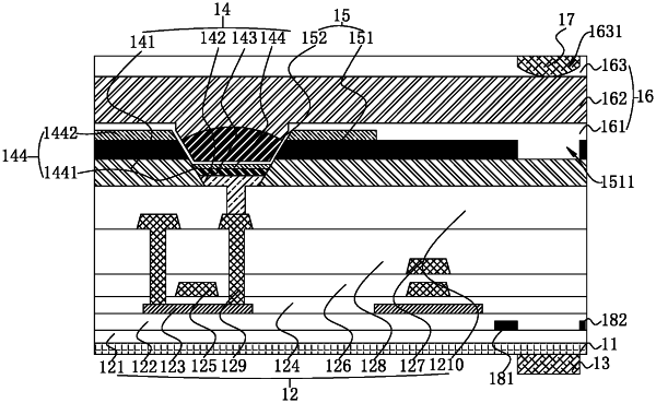
a thin-film encapsulation layer disposed on the color filter layer, and the thin-film encapsulation layer comprising a first inorganic encapsulation layer, an organic encapsulation layer, and a second inorganic encapsulation layer stacked from bottom to top, wherein a first via-hole is formed in a surface of the second inorganic encapsulation layer, the first via-hole penetrates the second inorganic encapsulation layer and exposes the organic encapsulation layer, and the first via-hole is positioned above the fingerprint recognition sensor;
a fingerprint recognition sensor disposed on a side of the flexible substrate away from a finger contact side to receive reflected light reflected by a fingerprint, and identify the fingerprint according to the reflected light;
wherein a collimator lens structure is embedded in the first via-hole, the collimator lens structure is configured to allow the reflected light reflected by the fingerprint converged on different directions and allow the reflected light reflected in a vertical direction converged on the fingerprint recognition sensor; the collimator lens structure is a collimator lens, and the collimator lens comprises a main optical axis, and the main optical axis extends in a vertical direction.
|