| CPC H10K 59/38 (2023.02) [H10K 59/1201 (2023.02); H10K 59/35 (2023.02); H10K 59/40 (2023.02); H10K 71/00 (2023.02)] | 9 Claims |
|
1. A display panel, comprising:
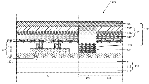
a thin-film transistor structure layer;
an organic light emitting diode (OLED) light-emitting layer disposed on the thin-film transistor structure layer, wherein the OLED light-emitting layer includes a first light-emitting color sub-pixel, a second light-emitting color sub-pixel, and a third light-emitting color sub-pixel that are arranged at intervals;
a touch layer disposed on the OLED light-emitting layer; and
a color filter including a first color film layer disposed on the first light-emitting color sub-pixel, and a color resist layer located near the first color film layer;
wherein the color resist layer includes the first color film layer disposed on the touch layer;
wherein the touch layer includes:
a planarization layer disposed on a side of an array substrate facing the color filter;
a first metal layer disposed on the planarization layer and including a first metal electrode been patterned;
an insulating layer disposed on the planarization layer and covering the first metal layer, wherein the first color film layer and the insulating layer are provided in a same layer; and
a second metal layer disposed on the insulating layer and including a second metal electrode been patterned, wherein the second metal electrode is connected to the first metal electrode, and the color resist layer is disposed on the second metal electrode;
wherein the display panel further includes an opening penetrating from a surface of the color resist layer to a surface of the first color film layer;
wherein the color filter further includes a protective layer filled in the opening and covering the color resist layer.
|