| CPC H10K 59/1315 (2023.02) [H10K 50/8426 (2023.02); H10K 71/00 (2023.02); H10K 59/1201 (2023.02)] | 18 Claims |
|
1. A display device comprising:
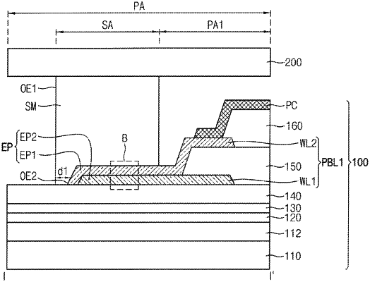
an array substrate comprising a pixel array disposed in a display area, the pixel array including a transistor and an organic light-emitting diode electrically connected to the transistor, the organic light-emitting diode including a first electrode, an organic light-emitting layer disposed on the first electrode and a second electrode disposed on the organic light-emitting layer, the transistor including an active pattern, a drain electrode disposed on the active pattern and a connection electrode disposed on the drain electrode and electrically connecting the drain electrode to the first electrode of the organic light-emitting diode;
an encapsulation substrate disposed to face the array substrate; and
a sealing member disposed in a sealing area, the sealing member disposed between the array substrate and the encapsulation substrate to combine the array substrate with the encapsulation substrate,
wherein the array substrate comprises:
an organic insulation layer disposed in a first peripheral area between the display area and the sealing area;
a power bus line disposed in the first peripheral area, the power bus line comprising a first wiring layer and a second wiring layer disposed on the first wiring layer, each of the first wiring layer and the second wiring layer overlapping the organic insulation layer; and
a compensation pattern disposed under the sealing member and extending along an outer edge of the sealing member, the compensation pattern comprising a first contiguous compensation layer and a second contiguous compensation layer, wherein:
the first compensation layer is connected to the first wiring layer, and
the second compensation layer is disposed on the first compensation layer in a same layer as the connection electrode and connected to the second wiring layer,
wherein the compensation pattern overlaps at least 50% of the sealing member, and
the compensation pattern has a first outer edge and the sealing member has a second outer edge spaced the first outer edge by about 100 μm to about 200 μm in a plan view.
|