| CPC H10K 59/131 (2023.02) [H10K 50/8426 (2023.02); H10K 71/00 (2023.02); H10K 59/1201 (2023.02)] | 15 Claims |
|
1. A display device comprising:
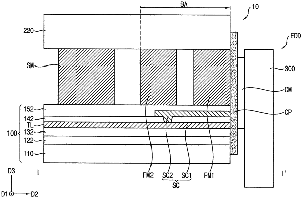
an array substrate including a pixel array disposed on a base substrate, a side terminal disposed on the base substrate, a transfer wiring electrically connected to the side terminal and the pixel array, and an inorganic insulation layer covering the side terminal;
a cover substrate coupled with the array substrate;
a seal disposed between the array substrate and the cover substrate and surrounding the pixel array;
a filler, spaced apart from the seal, the filler substantially consisting of an inorganic material overlapping at least a portion of the side terminal and filling a space between the array substrate and the cover substrate; and
a conductive connection pad disposed on a side surface of the array substrate and contacting the side terminal,
wherein the filler comprises a first filling member and a second filling member disposed between the first filling member and the seal, wherein the first filling member is separately disposed from the second filling member with a first air gap provided therebetween, wherein the first filling member and the second filling member are disposed along only a side of the array substrate where the side terminal is disposed,
wherein the first filling member has an outer side surface continuously connected to an outer side surface of the inorganic insulation layer and contacting the conductive connection pad,
wherein the side terminal includes an upper conductive layer and a lower conductive layer disposed under the upper conductive layer with an intervening layer between the upper conductive layer and the lower conductive layer, and
wherein both of the upper conductive layer and the lower conductive layer contact the conductive connection pad.
|