| CPC H10K 59/131 (2023.02) [H01L 27/1237 (2013.01); H01L 27/124 (2013.01); H01L 29/78672 (2013.01); H10K 59/124 (2023.02); H10K 59/126 (2023.02)] | 12 Claims |
|
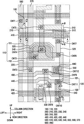
1. A display device comprising:
a substrate;
a first semiconductor layer on a surface of the substrate;
a first scan line above the first semiconductor layer;
a second semiconductor layer above the first scan line;
a second scan line above the second semiconductor layer;
a first transistor configured to control a driving current flowing from a first electrode of the first transistor to a second electrode of the first transistor according to a voltage applied to a gate electrode of the first transistor;
a light-emitting element electrically coupled to the second electrode of the first transistor and configured to emit light according to the driving current;
a second transistor electrically coupled to the first electrode of the first transistor and configured to transfer a data voltage;
the first semiconductor layer forming channel regions of the first transistor and the second transistor;
the first scan line electrically coupled to a gate electrode of the second transistor and extending in a first direction;
a third transistor configured to supply a voltage to the gate electrode of the first transistor, and including a first electrode electrically coupled to the second electrode of the first transistor and a second electrode electrically coupled to the gate electrode of the first transistor;
the second semiconductor layer forming a channel region of the third transistor; and
the second scan line electrically coupled to a gate electrode of the third transistor and extending in the first direction,
wherein the second scan line overlaps the first scan line in a second direction perpendicular to the surface of the substrate,
wherein the channel region of the third transistor overlaps between the first scan line and the second scan line in the second direction,
wherein the first scan line is configured to supply a first scan signal to the gate electrode of the second transistor, and the second scan line is configured to supply a second scan signal to the gate electrode of the third transistor, the second scan signal being different from the first scan signal, and
wherein the first and second scan lines are separately coupled to a scan driver to allow the first scan signal and the second scan signal to be independently supplied to the respective gate electrodes of the second and third transistors.
|