| CPC H10K 59/124 (2023.02) [H10K 50/865 (2023.02); H10K 59/122 (2023.02); H10K 59/123 (2023.02); H10K 59/131 (2023.02); H10K 59/1315 (2023.02)] | 24 Claims |
|
1. A display device comprising:
a substrate;
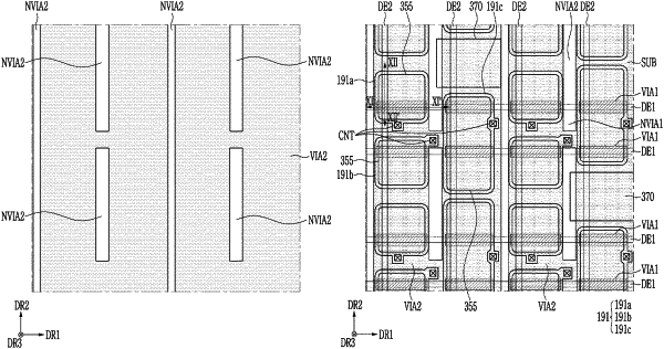
a plurality of first wires extending along a first direction on the substrate;
a first insulating layer disposed on the plurality of first wires;
a plurality of second wires disposed on the first insulating layer and extending along a second direction crossing the first direction;
a second insulating layer disposed on the plurality of second wires; and
a plurality of pixel electrodes disposed on the second insulating layer,
wherein the second insulating layer includes a plurality of first removed regions each extending along the second direction, a length of each of the plurality of first removed regions along the second direction being longer than a length of at least one of the plurality of pixel electrodes along the second direction and a width of each of the plurality of first removed regions along the first direction being shorter than a width of at least one of the plurality of pixel electrodes along the first direction.
|