| CPC H10K 59/122 (2023.02) [H10K 50/844 (2023.02); H10K 59/131 (2023.02)] | 18 Claims |
|
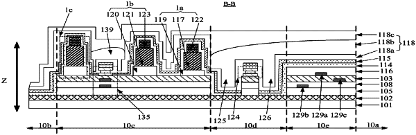
1. A display substrate comprising a display area, an opening area, and a transition area between the display area and the opening area, the transition area being disposed around the opening area; wherein the display substrate comprises:
a base substrate;
a drive circuit layer formed on the base substrate, and comprising an interlayer dielectric layer at the display area and the transition area;
display parts located at the display area, and comprising a first electrode and a pixel definition portion sequentially formed on the interlayer dielectric layer;
a first packaging dam located at the transition area and disposed around the opening area, wherein the first packaging dam comprises a first protective portion and a first blocking portion sequentially laminated on the interlayer dielectric layer;
a second packaging dam located at the transition area and disposed around the opening area, wherein the second packaging dam is at a side of the first packaging dam far away from the display area, a thickness of the second packaging dam is greater than a thickness of the first packaging dam, and the second packaging dam comprises a second protective portion and a second blocking portion sequentially laminated on the interlayer dielectric layer; wherein
the first blocking portion, the second blocking portion, and the pixel definition portion are arranged on the same layer, and are disconnected from each other;
a distance between the first packaging dam and the second packaging dam is less than a distance between the first packaging dam and the display area;
at least one of the first packaging dam and the second packaging dam further comprises a photo spacer formed at a side of the first blocking portion or the second blocking portion back away from the interlayer dielectric layer; and
the display parts further comprise a supporting portion formed at a side of the pixel definition portion back away from the base substrate, the supporting portion and the photo spacer are arranged on the same layer.
|