| CPC H10K 59/122 (2023.02) [H10K 50/824 (2023.02); H10K 71/00 (2023.02); H10K 2102/103 (2023.02)] | 9 Claims |
|
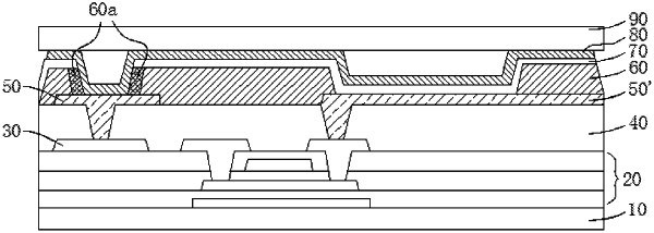
1. A display panel, comprising:
a substrate;
an array layer disposed on the substrate;
a patterned first auxiliary cathode layer disposed on the array layer;
a planarization layer disposed on the first auxiliary cathode layer;
a patterned second auxiliary cathode layer and an anode layer both disposed on the planarization layer, wherein the second auxiliary cathode layer is electrically connected to the first auxiliary cathode layer through a via hole;
a pixel definition layer disposed on the second auxiliary cathode layer and provided with a pixel opening and a connecting hole corresponding to the second auxiliary cathode layer, wherein the pixel definition layer is a hydrophilic material;
an organic light-emitting layer disposed on the pixel definition layer, wherein the second auxiliary cathode layer is exposed to the connecting hole through the organic light-emitting layer; and
a cathode layer disposed on the organic light-emitting layer and electrically connected to the second auxiliary cathode layer through the connecting hole, wherein an entire inner surface of the connecting hole is covered by and completely directly contacts the cathode layer, and each of the second auxiliary cathode layer and the first auxiliary cathode layer has a sheet resistance lower than a sheet resistance of the cathode layer,
wherein the pixel definition layer comprises an organic light-emitting material infiltration portion in a peripheral area of the connecting hole, and the organic light-emitting material infiltration portion contains a material for formation of the organic light-emitting layer.
|