| CPC H10K 59/1213 (2023.02) [G09G 3/3233 (2013.01); H01L 27/1222 (2013.01); H01L 27/1225 (2013.01); H10K 59/123 (2023.02); H10K 59/131 (2023.02); G09G 2300/0814 (2013.01); G09G 2300/0819 (2013.01); G09G 2300/0861 (2013.01); G09G 2310/0248 (2013.01); G09G 2310/0286 (2013.01); G09G 2310/061 (2013.01); G09G 2310/08 (2013.01)] | 21 Claims |
|
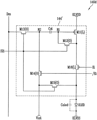
1. A pixel, comprising:
an organic light emitting diode;
a first transistor having a first electrode coupled to a first node and a second electrode coupled to an anode electrode of the organic light emitting diode, the first transistor to control an amount of driving current flowing from a first driving power supply (ELVDD) coupled to the first node to a second driving power supply (ELVSS) through the organic light emitting diode;
a second transistor coupled between a data line and the first node, and a gate electrode of the second transistor coupled to a first scan line;
a third transistor coupled between a gate electrode and the second electrode of the first transistor, and a gate electrode of the third transistor coupled to a second scan line, wherein
each of the first transistor and the second transistor includes an active layer including polysilicon,
the third transistor include an active layer including an oxide semiconductor material, and
a first scan signal sun lied to the first scan line and a second scan signal supplied to the second scan line are set to signals laving opposite polarities and overlapping.
|