| CPC H10K 59/1213 (2023.02) [H10K 71/00 (2023.02); H01L 27/1222 (2013.01); H01L 29/4908 (2013.01); H01L 29/78645 (2013.01); H01L 29/78675 (2013.01); H10K 59/1201 (2023.02)] | 20 Claims |
|
1. A display device comprising:
a substrate;
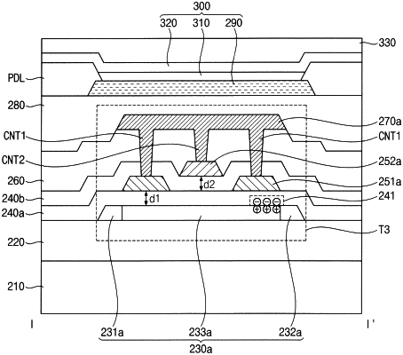
a first active layer disposed on the substrate and including a first source region, a first drain region, and a first channel region disposed between the first source region and the first drain region;
a first gate insulating layer covering the first active layer on the substrate;
first gate electrodes respectively disposed on opposite sides of the first channel region and disposed directly on an upper surface defining the first gate insulating layer;
a second gate insulating layer covering the first gate electrodes and disposed on the first gate insulating layer;
a second gate electrode disposed in a central portion of the first channel region and disposed directly on an upper surface defining the second gate insulating layer; and
a first connection electrode disposed on the second gate electrode and connected to the first and second gate electrodes.
|