| CPC H10K 50/844 (2023.02) [H10K 59/122 (2023.02); H10K 59/124 (2023.02); H10K 71/00 (2023.02); H10K 77/10 (2023.02); H10K 59/1201 (2023.02)] | 26 Claims |
|
1. A display panel comprising:
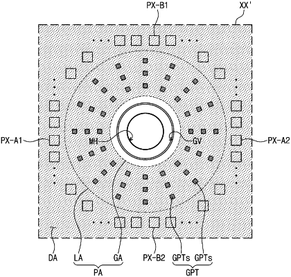
a base substrate including a front surface and a rear surface, wherein a hole area, an active area surrounding the hole area, and a peripheral area adjacent to the active area are defined in the base substrate, and a through-hole defined through the base substrate from the front surface to the rear surface and a groove part surrounding the through-hole and recessed from the front surface are defined in the hole area;
a circuit layer comprising a first circuit insulating layer disposed on the base substrate, a second circuit insulating layer disposed on the first circuit insulating layer, and a thin film transistor disposed on the active area;
a display layer comprising a first display insulating layer disposed on the circuit layer, a second display insulating layer disposed on the first display insulating layer, and a light emitting element disposed on the active area and connected to the thin film transistor;
a guide pattern disposed on the circuit layer and disposed between the active area and the through-hole; and
an encapsulation layer which covers the light emitting element, wherein the encapsulation layer comprises a first inorganic layer disposed on the active area and the hole area, a second inorganic layer disposed on the first inorganic layer, and an organic layer disposed between the first inorganic layer and the second inorganic layer,
wherein the organic layer covers at least a portion of the guide pattern in a plan view.
|